SHAKESPEARE’s Guide on PCB Manufacturing From Kenya
“Give every man thy ear, but few thy voice.”
William Shakespeare
Shakespeare’s guide on Printed Circuit Board (PCB) Manufacturing from Kenya is a comprehensive explanation of manufacturing printed circuit boards. The guide discusses the various steps involved in the process, from the initial design to the testing of the finished product. This guide is important because it helps people in Kenya understand what PCB manufacturing entails and how they can start with this process.
The PCB manufacturing process is critical for the assembly of electronic devices and circuits. PCBs are used to support and connect electronic components using conductive tracks, pads and features etched from copper sheets laminated onto a non-conductive substrate.
The manufacturing process is important because it determines the quality and reliability of the finished product. Poorly manufactured PCBs can cause electrical shorts, signal integrity issues and intermittent failures.

Introduction: Why is the PCB Manufacturing Process Important?
If you are an electronics enthusiast, like I am, you know that one of the products that is close to our heart is a PCB. PCBs are just beautiful to look at. With the different layers, you will be able to create different animations on your PCB.
This picture paints an image of how PCBs can be turned into art. But today we will not be talking about making art from PCBs.
There are many steps involved in the acquisition of a manufactured PCB from China to Kenya, and today I will show you how we will be shipping one.
What are the Steps Required in the PCB Manufacturing Process?
For our example, I will try and ship the TanaBoard. This is a development board based on the RP2040 chip. It is designed and assembled here in Kenya and I will show you how one can be imported.
1. Create a PCB design file from a concept.
Your creativity starts to parachute as soon as your concept is turned into a PCB design file. Reasonable PCB design is the foundation of PCB service. It is preferable to provide your Gerber file as it is the industry standard rather than the CAD files to prevent risks that could cause plagiarism and misunderstandings between two parties, you (customers) and PCB manufacturers.
2. Choose a dependable Chinese PCB maker or assembler.
There are many ways to assess a PCB maker or PCB assembler. Because there are so many fabless PCB brokers and PCB manufacturers in China, I think this step is the most difficult in the acquisition of China’s PCB service. Your PCB service is halfway complete once you’ve chosen a reputable PCB manufacturer.
I would recommend SeedStudio followed by JLCPCB as I have worked with both. For this, I will be going with JLCPCB as I had previously done an article using SeeedStudio here
3. Submit your Gerber files to the PCB manufacturer.
Make sure you have an account on the website. Log in and head over to Order Now.
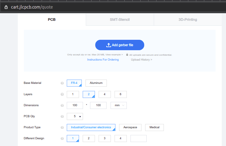
Upload your Gerber files and select the necessary parameters for your PCB.
In our case, we will be using:
- Base Material — FR4
- Layers — Are generated automatically from your Gerber files
- Dimensions — Are generated automatically from your Gerber files
- PCB Qty — Depends on your quantity but choose 5
- Product Type — Industrial/Consumer electronics
- Different Design — One
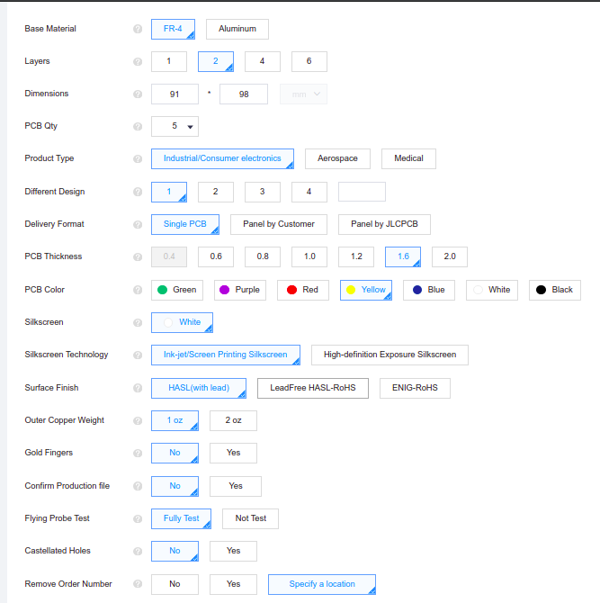
- Delivery Format — Single
- PCB Thickness — 1.6mm
- PCB Color — Any of your choice
- Silkscreen — White
- Silkscreen Technology — Inkjet/Screen Printing Silkscreen
- Surface Finish — I would recommend ENIG-RoHS as it is unleaded but HASL(with lead) is cheaper
- Outer Copper Weight — 1oz
- Gold Fingers — No
- Confirm Production file — No
- Flying Probe Test — Fully test
- Castellated Holes — No
- Remove Order Number — Specify a location (Make sure you added JLCJLCJLCJLC on your PCB on the silkscreen)
Since we will also be assembling it ourselves you choose Order together with Stencil. For the stencil, you can leave it as it is.

4. Make the order
Save to cart the order. Then view your Cart and make the checkout.
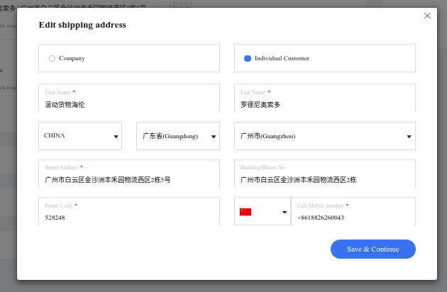
5. Shipping and billing information
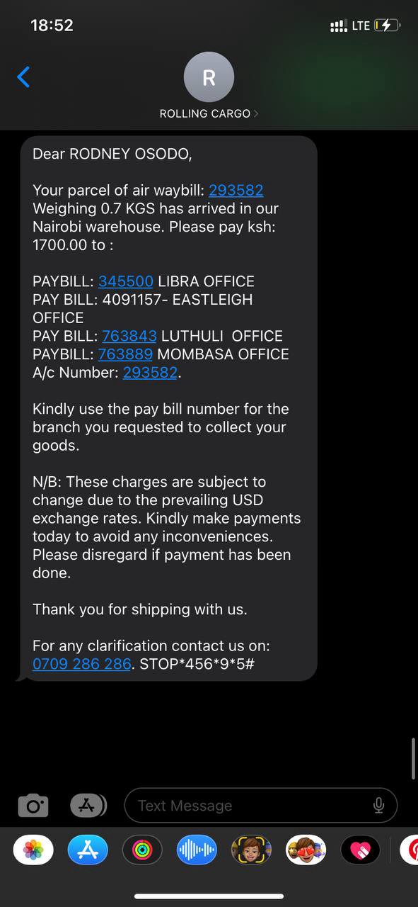
We will be using Rolling Cargo as a courier service. DHL is expensive and FedEx takes a long to deliver your package. On the Shipping Information change:
- Ship to Individual Customer
- First name : 滚动货物海伦
- Last name : Your name in Chinese e.g 罗德尼奥索多
- Country : China
- Province : Guangdong
- Sub provincial City : Guangzhou
- Street Address : 广州市白云区金沙洲丰禾园物流西区2栋5号
- Building House Number : 广州市白云区金沙洲丰禾园物流西区2栋
- Postal Code : 528248
- Cell Mobile Number : +8618826260043
You can change your billing information or leave it the same as the shipping address.
Choose SF Express (Within Guangdong) as your shipping method; it takes 3 business days.
6. Payment
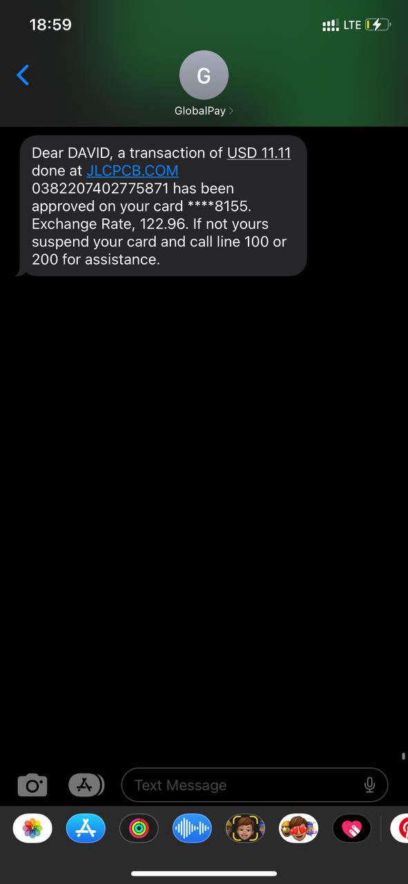
We will take advantage of the fact that Mpesa is Global. Change to Credit Card / Debit Card and add your Mpesa GlobalPay details.
How Much Does it Cost to Manufacture PCBs in China?
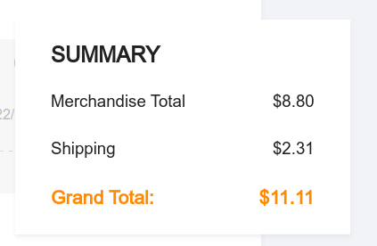
The PCBs now cost $11.11. You can reduce your price by not selecting stencil if you don’t need it. This will drop to $4.31.
Since our shipping is 1kg rolling cargo will charge us Ksh 1700. They usually charge 1700 per kg below 1kg and $1.3 per kg above 1kg.
Timeline
For green PCBs, it usually takes 1 day to complete while the others take an extra 1 day. So that is 2 days for PCB manufacturing. Shipping within China will take 3 business days and Shipping to Kenya will take 10–14 days. In total, it will take approximately 3 weeks for PCBs to arrive in Kenya
If you liked this article, click the👏 multiple times below so other people will see it here on Medium.
Let’s be friends on Twitter. Happy Coding 😉